Are you curious to know what is reverse bias? You have come to the right place as I am going to tell you everything about reverse bias in a very simple explanation. Without further discussion let’s begin to know what is reverse bias?
In the intricate realm of electronics, the phenomenon of reverse bias stands as a fundamental concept that shapes the behavior and functionality of semiconductor devices. Let’s delve into the essence of reverse bias, its implications in electronic components, and the role it plays in controlling the flow of current within semiconductor materials.
What Is Reverse Bias?
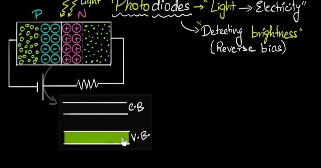
Reverse bias refers to the condition in which a voltage is applied across a semiconductor device, such as a diode or a transistor, in a manner that opposes the natural flow of current. This means the voltage polarity is opposite to the direction that facilitates current flow through the device in its forward-biased state.
Operation And Characteristics
- Blocking Current Flow: When a semiconductor device is under reverse bias, the applied voltage creates a depletion region within the device, widening the barrier for the flow of charge carriers (electrons or holes), inhibiting the movement of current.
- Minimal Leakage Current: While reverse bias prevents significant current flow, a small amount of leakage current may still occur due to minority carriers crossing the depletion region, but this current is typically negligible compared to forward bias conditions.
- Breakdown Voltage: If the reverse bias voltage exceeds a critical value known as the breakdown voltage, a phenomenon called reverse breakdown occurs, leading to a sudden increase in current and potential device damage.
Applications And Significance
- Diode Functionality: Reverse bias plays a crucial role in semiconductor diodes, allowing them to act as rectifiers by blocking the flow of current in one direction while permitting it in the other. This property enables the conversion of alternating current (AC) to direct current (DC) in rectification circuits.
- Transistor Operation: In transistors, the reverse bias condition across certain regions regulates the device’s behavior, enabling precise control over amplification and switching functions in electronic circuits.
Protection And Control
- Component Protection: Reverse bias conditions can protect semiconductor devices from excessive currents and overvoltage, safeguarding them against damage in electronic circuits.
- Signal Control: Reverse biasing certain regions of semiconductor devices aids in signal modulation and control, allowing for efficient signal processing in various electronic applications.
Conclusion
Reverse bias, a fundamental principle in semiconductor physics, governs the behavior and functionality of crucial electronic components. Its role in regulating current flow, controlling device operation, and ensuring component protection underscores its significance in the design and functionality of semiconductor devices, enabling the development of innovative and efficient electronic systems.
FAQ
What Is The Forward Bias?
Forward bias or biasing is where the external voltage is delivered across the P-N junction diode. In a forward bias setup, the P-side of the diode is attached to the positive terminal, and N-side is fixed to the negative side of the battery. Here, the applied voltage is opposite to the junction barrier potential.
Which Current Is In Reverse Bias?
It is seen that in a reverse-biased diode, some current flows through the depletion region. This current is called leakage current. Leakage current is dependent on minority current carriers. the minority carriers are electrons in the P type material and holes in the N type material.
What Is Forward Bias And Reverse Bias In Vedantu?
A diode acts as a closed switch when it is forward biased and allows the current to flow through it. In the reverse bias condition, a diode acts as an open switch and does not allow current to flow through it. An LED is always forward biased.
What Is Reverse Bias In Jfet?
JFETs are normally-on (normally-saturated) devices. The application of a reverse-biasing voltage between gate and source causes the depletion region of that junction to expand, thereby “pinching off” the channel between source and drain through which the controlled current travels.
I Have Covered All The Following Queries And Topics In The Above Article
What Is Forward Bias And Reverse Bias
What Is Reverse Bias
What Is Reverse Bias And Forward Bias
What Is Forward And Reverse Bias
What Is Reverse Bias


